Stanford researchers stretch a thin crystal to get better solar cells
Crystalline semiconductors like silicon can catch photons and convert their energy into electron flows. New research shows a little stretching could give one of silicon's lesser-known cousins its own place in the sun.

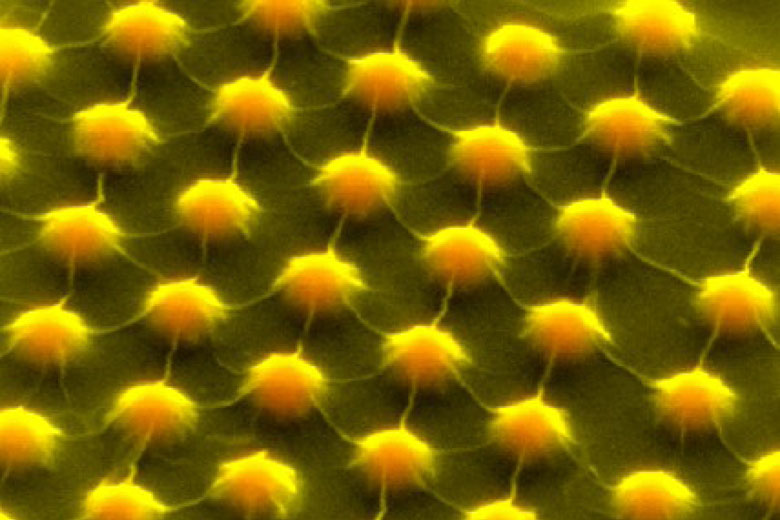
Colorized image, enlarged 100,000 times, shows an ultrathin layer of molybdenum disulfide stretched over the peaks and valleys of part of an electronic device. Just 3 atoms thick, this semiconductor material is stretched in ways to enhance its electronic potential to catch solar energy. (Image credit: Hong Li)
Nature loves crystals. Salt, snowflakes and quartz are three examples of crystals – materials characterized by the lattice-like arrangement of their atoms and molecules.
Industry loves crystals, too. Electronics are based on a special family of crystals known as semiconductors, most famously silicon.
To make semiconductors useful, engineers must tweak their crystalline lattice in subtle ways to start and stop the flow of electrons.
Semiconductor engineers must know precisely how much energy it takes to move electrons in a crystal lattice.
This energy measure is the band gap. Semiconductor materials like silicon, gallium arsenide and germanium each have a band gap unique to their crystalline lattice. This energy measure helps determine which material is best for which electronic task.
Now an interdisciplinary team at Stanford has made a semiconductor crystal with a variable band gap. Among other potential uses, this variable semiconductor could lead to solar cells that absorb more energy from the sun by being sensitive to a broader spectrum of light.
The material itself is not new. Molybdenum disulfide, or MoS2, is a rocky crystal, like quartz, that is refined for use as a catalyst and a lubricant.
But in Nature Communications, Stanford mechanical engineer Xiaolin Zheng and physicist Hari Manoharan proved that MoS2 has some useful and unique electronic properties that derive from how this crystal forms its lattice.
Molybdenum disulfide is what scientists call a monolayer: A molybdenum atom links to two sulfurs in a triangular lattice that repeats sideways like a sheet of paper. The rock found in nature consists of many such monolayers stacked like a ream of paper. Each MoS2 monolayer has semiconductor potential.
“From a mechanical engineering standpoint, monolayer MoS2 is fascinating because its lattice can be greatly stretched without breaking,” Zheng said.
By stretching the lattice, the Stanford researchers were able to shift the atoms in the monolayer. Those shifts changed the energy required to move electrons. Stretching the monolayer made MoS2 something new to science and potentially useful in electronics: an artificial crystal with a variable band gap.
“With a single, atomically thin semiconductor material we can get a wide range of band gaps,” Manoharan said. “We think this will have broad ramifications in sensing, solar power and other electronics.”
Scientists have been fascinated with monolayers since the Nobel Prize-winning discovery of graphene, a lattice made from a single layer of carbon atoms laid flat like a sheet of paper.
In 2012, nuclear and materials scientists at MIT devised a theory that involved the semiconductor potential of monolayer MoS2. With any semiconductor, engineers must tweak its lattice in some way to switch electron flows on and off. With silicon, the tweak involves introducing slight chemical impurities into the lattice.
In their simulation, the MIT researchers tweaked MoS2 by stretching its lattice. Using virtual pins, they poked a monolayer to create nanoscopic funnels, stretching the lattice and, theoretically, altering MoS2‘s band gap.
Band gap measures how much energy it takes to move an electron. The simulation suggested the funnel would strain the lattice the most at the point of the pin, creating a variety of band gaps from the bottom to the top of the monolayer.
The MIT researchers theorized that the funnel would be a great solar energy collector, capturing more sunlight across a wide swath of energy frequencies.
When Stanford postdoctoral scholar Hong Li joined the mechanical engineering department in 2013, he brought this idea to Zheng. She led the Stanford team that ended up proving all of this by literally standing the MIT theory on its head.
Instead of poking down with imaginary pins, the Stanford team stretched the MoS2 lattice by thrusting up from below. They did this – for real rather than in simulation – by creating an artificial landscape of hills and valleys underneath the monolayer.
They created this artificial landscape on a silicon chip, a material they chose not for its electronic properties, but because engineers know how to sculpt it in exquisite detail. They etched hills and valleys onto the silicon. Then they bathed their nanoscape with an industrial fluid and laid a monolayer of MoS2 on top.
Evaporation did the rest, pulling the semiconductor lattice down into the valleys and stretching it over the hills.
Alex Contryman, a PhD student in applied physics in Manoharan’s lab, used scanning tunneling microscopy to determine the positions of the atoms in this artificial crystal. He also measured the variable band gap that resulted from straining the lattice this way.
The MIT theorists and specialists from Rice University and Texas A&M University contributed to the Nature Communications paper.
Team members believe this experiment sets the stage for further innovation on artificial crystals.
“One of the most exciting things about our process is that is scalable,” Zheng said. “From an industrial standpoint, MoS2 is cheap to make.”
Added Manoharan: “It will be interesting to see where the community takes this.”
